Printable NTC Sensor
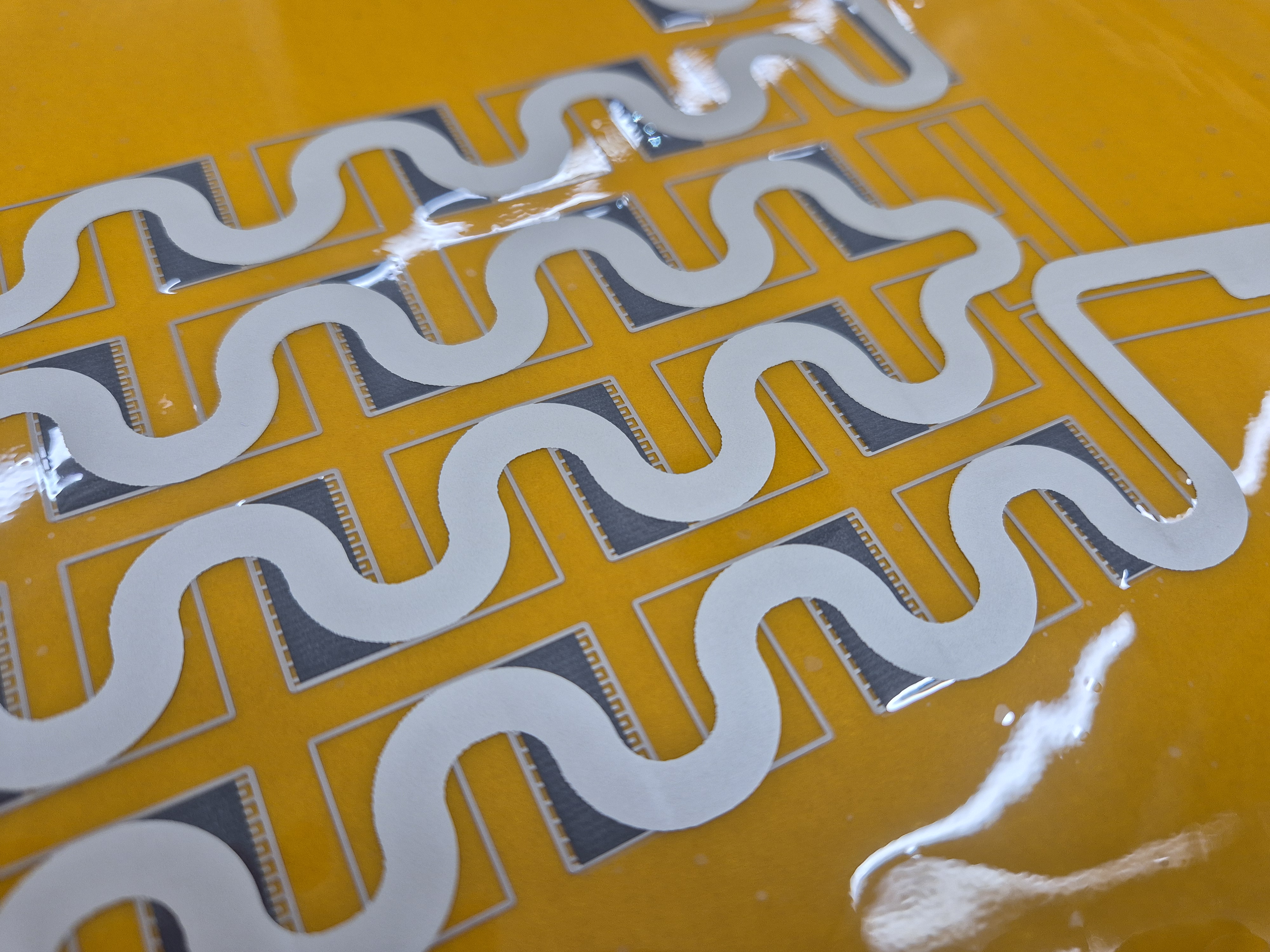
Printed NTC temperature sensor on thin foil substrates — printed sensors for surface-integrated measurement, thermal validation and hotspot detection in limited spaces.
Challenge
Conventional SMD temperature sensors work well in many electronics assemblies, but they are not ideal for every thermal measurement task. They add component height, need mechanical placement and soldering, and can be difficult to integrate between cells, inside thin material stacks or across functional surfaces. Engineers searching for a printed temperature sensor, a temperature sensor on foil or a thin NTC sensor usually need thermal data closer to the surface: for validation, hotspot detection, functional surfaces or battery cell/module monitoring. In some applications, temperature and mechanical pressure can change at the same time — for example when battery cells expand during charging or aging. In these cases, the sensing concept must fit the available space, surface geometry, substrate and readout electronics.
Our Solution
ATT's Printable NTC Sensor is a screen-printed temperature sensing layer based on ceramic NTC particles. It can be integrated as a very thin functional film on suitable foil or rigid substrates, with typical dry film thicknesses in the range of 20–30 μm depending on the final stack-up. The printed layout can be designed as a point sensor, an array, a strip or a hotspot-sensitive geometry. This makes it especially interesting for locations where conventional sensor packages are too high, too slow thermally or too difficult to integrate. For SEO and engineering clarity: it is not a generic thermal camera, but an application-specific printed NTC temperature sensor concept for surface measurement, thermal validation and integrated control. The final sensor concept considers resistance target, B-value, substrate, encapsulation, calibration and readout architecture from the beginning.
How It Works
Application & Measurement Concept
We first clarify the temperature range, available installation space, mechanical pressure situation, substrate, environmental exposure and readout electronics. This defines whether a point sensor, array, strip or hotspot-sensitive geometry is the right approach.
Printed NTC Layout
The NTC material is screen-printed on a suitable high-temperature-stable substrate such as polyimide or ceramic. Electrode layout, sensor area and resistance target are adapted to the application instead of using a fixed component package.
Protection & Integration
Depending on the environment, the sensor can be combined with a cover layer, encapsulation or barrier concept. This is important when humidity, liquids, lamination, molding or long-term stability have to be considered.
Characterization & Calibration
The printed sensors are electrically characterized. For precision applications, conditioning, calibration or trimming concepts can be used to align the resistance-temperature behavior with the required measurement accuracy.
Application Areas
Battery Cell & Module Monitoring
Thin printed temperature sensors can be placed in locations where component height matters, such as between cells or on battery surfaces. The concept is especially relevant when temperature and mechanical pressure changes must be considered separately.
Hotspot Detection on Surfaces
Printed strip or area geometries can be designed to react strongly to local hot spots. This allows larger surfaces to be monitored with fewer measurement channels than a dense array of individual point sensors.
Thermal Mapping & Sensor Arrays
Arrays of printed NTC elements can help measure temperature fields in development, validation and process-monitoring setups. Multiplexing concepts can reduce the number of external connections.
Thin Functional Surfaces
Printed NTC layers can be integrated into foils, heated surfaces, plastic parts or material stacks where a conventional sensor package would be visible, too thick or thermally too slow.
Technical Data
Key Advantages
- Very thin printed temperature sensing layer for constrained installation spaces
- Designed to reduce pressure-related influence on the temperature signal
- Configurable as point sensors, arrays, strips or hotspot-sensitive geometries
- Suitable for printed temperature sensor on foil and surface-integrated sensing concepts
- Low thermal mass can support fast response when the stack-up is designed accordingly
- Resistance target and B-value can be adapted within the limits of the material and readout concept
- Encapsulation, calibration and readout architecture are considered application by application
- Patent-protected ATT technology based on printed ceramic NTC particles
Frequently Asked Questions
What is a printed temperature sensor on foil?
How is a printed NTC sensor different from a traditional SMD NTC?
Why is pressure influence important for temperature sensing?
Can the sensor be used for hotspot detection?
What accuracy can be achieved?
Does the sensor need encapsulation?
Is the Printable NTC Sensor a direct replacement for every SMD temperature sensor?
Let's Start Your Project
Ready for the next generation of thermal solutions? Contact our expert team.
Response within 24 hours • Free initial consultation